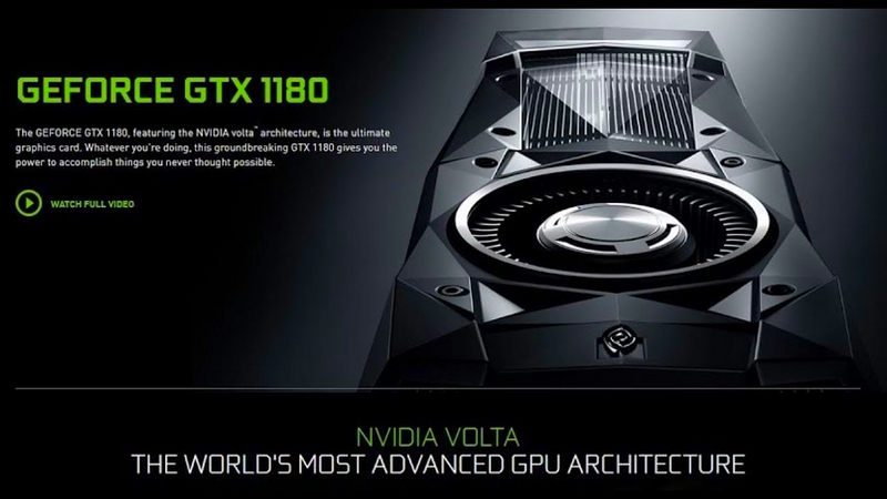
It’s been a while since Nvidia introduced its last new graphics architecture for gaming GPUs—more than two years to be precise. That last architecture was Pascal, and it has powered everything from the top-tier GTX 1080 and GTX 1080 Ti to the entry level GTX 1050 and GT 1030. The next generation of Nvidia graphics cards is finally approaching, using the Turing architecture. Here’s what we know about the GTX 1180, what we expect in terms of price, specs, and release date, and the winding path we’ve traveled between Pascal and Turing.
The things we ‘know’ about GTX 1180
The list of things that we know—that we’re absolutely certain are correct—can basically be summarized into a single word: nothing. Nvidia has been extremely tight-lipped about its future GPUs this round, and we’re not even sure about the name. Rumors of GTX 1180 and GTX 2080 have been swirling for months, though it looks like the 1180 is going to win out on the official name. We’re going to stick with 1180 for the remainder of this piece and are confident enough of the name that it’s ensconced in a cheap photoshop above. (Expect a hasty update if the winds of change start gusting.) We’re also not sure what the codename for these new chips will be—GT104 would be an easy choice, but Nvidia had GT part names with the Tesla architecture back in the GTX 280 days (2008-2009). Those were all GT200 labels, though, so GT100 could still happen.
While Nvidia hasn’t officially revealed anything, we’re 99 percent certain on three things. First, the next generation architecture is codenamed Turing. Second, it will be manufactured using TSMC’s 12nm FinFET process. (We may see some Turing GPUs manufactured by Samsung later, as was the case with the GTX 1050/1050 Ti and GT 1030 Pascal parts, but the initial parts will come from TSMC.) Third, the first Turing graphics cards will use GDDR6 memory—not HBM2, due to costs and other factors, but GDDR6 will deliver higher performance than the current GDDR5X. Let’s hit those last two in a bit more detail.
What does the move to 12nm from 16nm mean in practice? Various sources indicate TSMC’s 12nm is more of a refinement and tweak to the existing 16nm rather than a true reduction in feature sizes. In that sense, 12nm is more of a marketing term than a true die shrink, but optimizations to the process technology over the past two years should help improve clockspeeds, chip density, and power use—the holy trinity of faster, smaller, and cooler running chips.
GDDR6 continues down the path graphics memory has traveled from GDDR5 and GDDR5X. Over its lifetime, GDDR5 has gone from 3.6 GT/s (that’s giga-transfers per second, though in practice it’s almost the same as Gbit/s) with AMD’s HD 4870 back in 2008, to 9 GT/s with the GTX 1060 6GB. GDDR5X has a range of 10-14 GT/s by sending more data per clock rather than higher clockspeeds. Where the base clock of the GTX 1070 GDDR5 is 2002MHz (8,008 MT/s effective), the GTX 1080 has a base clock of 1251MHz and sends twice as much data per clock (10,008 MT/s effective). Micron ended up being the only company to produce GDDR5X, with Nvidia being the only consumer running GDDR5X at 11 GT/s. GDDR6 will see far broader support, with Micron, Samsung, and SK-Hynix all participating. GDDR6 has an official target range of 14-16 GT/s, and Micron is already showing 18 GT/s modules. GTX 1180 cards are likely to use faster GDDR6, but the exact clockspeeds remain a question mark.


 (No Ratings Yet)
Related articles

Warcraft: Wrath of the Lich King
Jul 06, 2024
RNCY Clan – CSGO2
Jun 30, 2024


Leave a Reply